- The Transistor of the University of Beijing could overcome Intel, TSMC and Samsung's superior silicon chips
- The full door coverage increases the speed and cuts the use of energy in the design of innovative Chinese transistors
- China may have jumped the US chips technology. With this innovation of transistors without silicon
Chinese researchers from the University of Beijing have announced what seems to be an advance in transistor design, which if marketed, could drastically change the direction of microprocessor development.
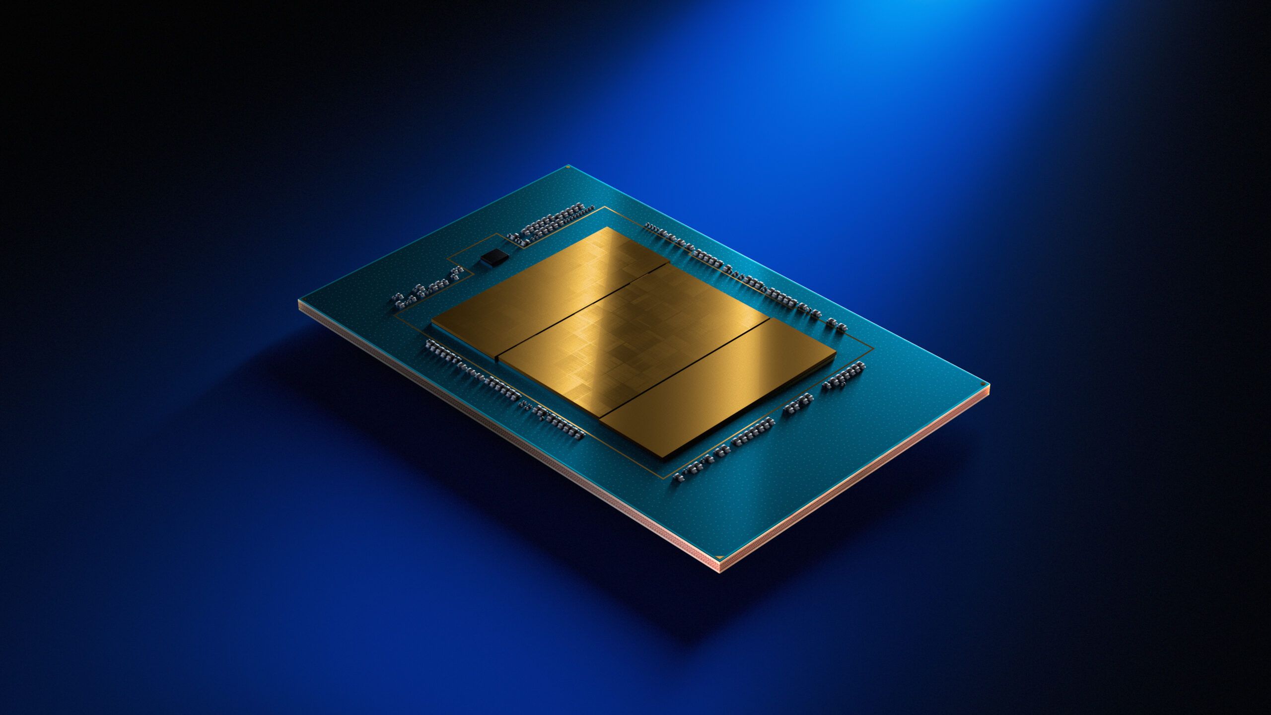
The team created a silicon transistor based on a two -dimensional material, Bismuth Oxyselenide.
Innovation depends on the Gate-Lall-Around architecture (GaaFet), where the transistor door is completely involved around the source. The traditional designs of Finfet, which dominate the current silicon -based processors, only allow the partial coverage of the door. This complete wrap structure improves the contact area between the door and the channel, improving performance by reducing energy leakage and allowing better current control.
Could this mark the end of silicon chips?
Posted in Nature materialsThe document suggests that the new 2D GAAFET could rival or even exceed silicon transistors both in speed and energy efficiency.
The researchers affirm that their 2D transistor achieves speeds for 40% faster than the last 3nm intell chips while using 10% less power, a performance that would place it ahead of current TSMC and Samsung processors.
The partial coverage of the door in traditional designs limits current control and increases energy loss. The new full door structure addresses these problems, which results in a large voltage gain and an ultra low power use. The team has already built small logical units using the new design.
“It is the fastest and most efficient transistor in history,” said Beijing University. These statements are backed by the tests carried out in identical conditions for those used for the main commercial chips.
“If the chips innovations based on existing materials are considered a 'shortcut', then our development of 2D transistors based on materials is similar to 'changing lanes,” said Professor Peng Hailin, the main scientist of the project.
Unlike the vertical structures of fingers, the new design resembles the intertwined bridges. This architectural change can exceed the limits of miniaturization facing silicon technology, especially when the industry pushes below the 3NM threshold. It could also benefit faster laptops that such compact chips require.
The team developed two new bismuth -based materials: bi₂o₂ be like the semiconductor and bi₂seo₅ as the dielectric door.
These materials have a low interface energy, reducing defects and electron dispersion.
“This allows electrons to flow almost without resistance, such as water through a smooth pipe,” Peg explained.
The performance results are backed by calculations of functional density theory (DFT) and validated through physical tests using a high precision manufacturing platform in PKU.
Researchers affirm that transistors can be manufactured using current semiconductor infrastructure, which simplifies future integration.